Fabrication of Poly(triaryl amine) Field-effect Transistors
![Poly[bis(4-phenyl)(2,4,6-trimethylphenyl)amine] Poly[bis(4-phenyl)(2,4,6-trimethylphenyl)amine]](/deepweb/assets/sigmaaldrich/marketing/global/images/technical-documents/protocols/materials-science-and-engineering/organic-electronics/fabrication-of-poly-structure.gif)
Poly[bis(4-phenyl)(2,4,6-trimethylphenyl)amine] is an amorphous p-type polymer semiconductor.1, 2 It may be used to fabricate field-effect transistors (FETs). PTAA is also useful as a hole transport material in organic light emitting diodes (OLEDs).
Precautions and Disclaimer
This product is for R&D use only, not for drug, household, or other uses. Please consult the Safety Data Sheet for information regarding hazards and safe handling practices.
Storage/Stability
Store the product at room temperature.
Procedure
Fabrication of PTAA field-effect transistors (FETs)
Bottom-gate bottom-contact FETs were fabricated in a nitrogen atmosphere on highly doped Si-wafers with a thermally grown 250 nm SiO2 layer. The two layers served as the gate electrode and gate insulator. Au source and drain electrodes (30 nm thick) were defined by standard photolithography:
channel length (L) = 10 mm
channel width (W) = 10 mm
Prior to deposition of the PTAA polymer layer, the Si-wafers were treated with octyltrichlorosilane (OTS-18, 104817 ) by immersing them in 10 mM solutions in toluene for 15 minutes at 60 °C.
A homogeneous solution of PTAA was prepared in toluene at room temperature containing 1.0 wt% of the polymer. This solution was deposited via spin-coating at 500 rpm for 30 seconds followed by 2,000 rpm for 50 seconds.
Results
Electrical characterization of the PTAA FETs was conducted in a nitrogen atmosphere with a HP4155B semiconductor parameter analyzer. Field-effect mobilities were calculated from transfer characteristics (saturation regime) employing the relation:3

Isd is the source-drain current (saturation regime)
Vg and Vsd gate and soxce-drain voltage, respectively
Ci the insulator capacitance
W and L the channel width and length
V0 the turn-on voltage
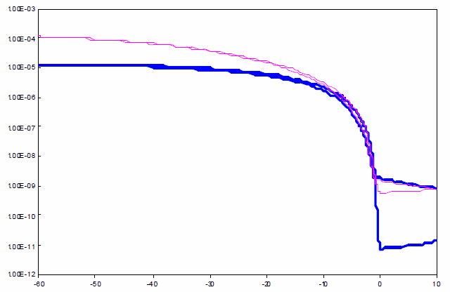
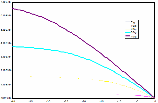
Transfer and output curves for PTAA transistors are shown in Figures 1 and 2.

Figure 1.Transfer output curves for PTAA transistors corresponding to field effect mobility of 4 x 10⁻³ cm2/Vs.

Figure 2.Output curves for PTAA transistors corresponding to field effect mobility of 4 x 10⁻³ cm2/Vs.
References
Data courtesy of Dr. Iain McCulloch, Imperial College London and Flexink, Inc.
To continue reading please sign in or create an account.
Don't Have An Account?