Nanoparticle Zinc Oxide ET Layers for Org. Photodet.
Introduction
Recent progress in the area of solution-processed functional materials has led to the development of a variety of thin-film optoelectronic devices with significant promise in the industrial and consumer electronics fields.1,2 These devices are becoming core technologies for the development of novel applications in sensing,3 energy harvesting,4 and energy conversion, exhibiting a unique combination of mechanical flexibility and light weight.5 Optical sensor research is growing in the area of organic photodiodes, with a special focus on the development of high-performance multilayer device architectures printed on a variety of substrates.6,7 We present the fabrication of printed organic photodiodes (OPDs) based on bulk-heterojunction (BHJ) active materials utilizing zinc oxide (ZnO) hole blocking layers deposited from nanoparticle (NP)-based ink. In contrast to sol gel or precursor-based layer deposition, the use of NPs offers great benefits with regard to processability and, in particular, the ability to precisely adjust the electronic and optical properties of the NPs without influence from the required conditions of thin film deposition.
Figures of Merit of Photodetectors
Organic BHJ photodetectors and solar cells generally have the same device architecture and material set. However, they differ in application focus which requires the optimization of different figures of merit. While solar cells are generally characterized by the short circuit current density (JSC), open circuit voltage (VOC), fill factor (FF), and device efficiency (η), photodiodes are characterized by the current On–Off ratio in reverse bias, specific detectivity (D*), bandwidth (BW), and spectral responsivity (SR). SR is given in amperes per watt (A/W) and is analogous to the external quantum efficiency (EQE) in solar cells, as seen in Equation 1:

where Iph is the generated photocurrent per wavelength λ, q is the electron charge, c the speed of light, and h the Planck constant.
Unlike solar cells, photodiodes are generally operated in reverse bias in order to achieve a larger collection of photo-excited carriers. The On–Off ratio of photodiodes is defined as the ratio between the measured current under illumination and dark conditions at a certain bias voltage. The dark current density (Jdark) can be used to estimate the electrical noise (Snoise), which is dominated by the shot noise of the OPDs, as seen in Equation 2. A lower Snoise compared to the obtained SR will result in a higher D* as evident from Equation 3. D* is a figure of merit of photodetectors which characterizes the smallest detectable signal of the device.

The dynamic response of the photodiode is characterized by its BW, which can be obtained by a transient photocurrent measurement or by varying the frequency of the excitation source. BW is usually defined by the cut-off frequency at –3 dB, which corresponds to a power drop of ~50%.
Results of Fully Printed Photodetectors
In practice, the main leverage for increasing the On–Off ratio and, consequently, D* of a photodetector is the reduction of the dark current. This can be achieved by introducing interlayers that selectively block electrons in the device architecture in order to avoid charge recombination at the active layer/electrode interface and simultaneously adjusting the energy levels of the electrode to the active material. ZnO NPs have shown exceptional electron transport properties within optoelectronic devices.8,9 The photodiodes presented in this work were fabricated in an inverted device architecture onto indium-doped tin oxide (ITO)-covered glass or PET substrates. The electron transport layer (ETL) using ZnO NP dispersions was fabricated by spin casting, inkjet printing, and aerosol printing. A thermal treatment at 120 °C for 5 minutes was applied to fully dry the ETL. The active material comprising P3HT (poly(3-hexylthiophene-2,5-diyl)) (Prod. Nos. 698997 and 698989) and PCBM ([6,6]-phenyl C61 butyric acid methyl ester) (Prod. No. 684457) diluted in dichlorobenzene (40 g/L) was blended in a ratio of 1:0.9 and was spin cast, resulting in a ~200 nm thick layer. A 20 nm thick poly(3,4- ethylenedioxythiophene) polystyrene sulfonate (PEDOT:PSS) layer was spin cast and used as the hole transport layer (HTL). Afterward, the samples were transferred to a nitrogen-filled glovebox and thermally treated at 145 °C for 15 minutes on a hotplate in order to remove humidity from the PEDOT:PSS layer and improve BHJ morphology.
The 100 nm thick silver top electrode was thermally evaporated through a shadow mask in a vacuum system with a base pressure of 10–7 mbar. For the aerosol-printed OPDs, an active layer of poly({4,8-bis[(2-ethylhexyl)oxy] benzo[1,2-b:4,5-b’]dithiophene-2,6-diyl}{3-fluoro-2-[(2-ethylhexyl)carbonyl] thieno[3,4-b]thiophenediyl}) (PTB7, Prod. No. 772410) was blended with [6,6]-Phenyl-C71-butyric acid methyl ester (PC70BM, Prod. No. 684465) using a ratio of 1:1.5 (10 g L–1 in 1,2-dichlorobenzene) with 3% volume of diiodooctane printed on top of a PEDOT:PSS/AZO cathode. The film was then dried in a vacuum (15 mbar) for 15 minutes. The conductive transparent top anode was aerosol-printed using a diluted PEDOT:PSS dispersion and finally dried in vacuum (15 mbar) in an antechamber, then transferred into a glovebox. All devices were encapsulated with an adhesive barrier foil to avoid the penetration of oxygen and moisture into the device.
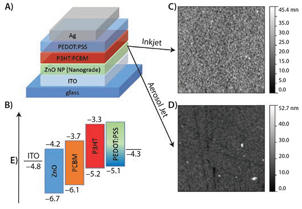
The OPD architecture and the relative energy level arrangement of the materials is shown in Figure 1A. Atomic force microscope (AFM) measurements were conducted on inkjet and aerosol-jet printed ZnO nanoparticle layers on ITO as shown in Figure 1B. Inkjet-printed ZnO using N11 Jet (Prod. No. 808202) formulation and aerosol-jet printed ZnO using N11 Slot produced the best results. Both techniques delivered a very homogeneous ZnO dense layer with a Root Mean Square (RMS) roughness on the order of 2.7 to 3 nm.

Figure 1. A)Inverted organic photodiode stack. B) Corresponding band diagram. AFM image (10 × 10 μm2) of C) inkjet-printed N11 Jet and D) aerosol-jet printed N11 Slot on ITOcovered glass.
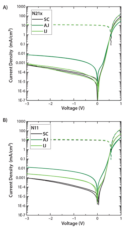
The J-V characteristic of devices with spin cast (SC), inkjet (IJ), and aerosol (AJ) printed A) aluminium-doped ZnO (AZO) and B) ZnO nanoparticlebased layers are presented in Figure 2. The device characteristics can be found in Table 1. A dark current density on the order of 10–4 mA/cm2 at –1 V was observed for the spin-cast AZO and ZnO layers, demonstrating the suitability of these ETLs for photodiode application. IJ-printed AZO layers show results as good as the spin-cast AZO layers; however, Jdark for AJ-printed ZnO, and IJ- or AJ-printed AZO-comprising devices is increased.

Figure 2.J-V curves of inverted stack comprising A) spin cast (SC) AZO (N21x), inkjet (IJ) (N21x Jet), and aerosol jet (AJ) (N21x slot) layers and B) for ZnO (N11, N11 Jet, N11 Slot), respectively.
This suggests that some low resistant pathways are formed during drying of the printed films. In both digital printing technologies, a sequential printing path is used. A local inhomogeneity of the surface energy on the ITO substrate can lead to incomplete wetting and even to pin holes in the ZnO layer. The layer thickness of the spin-cast ZnO and AZO layers is ~30 nm, while the necessary thickness of the IJ and AJP ZnO/AJP layers is below 50 nm. In the case of inkjet printing, the layer thickness was adjusted by the drop spacing or the NP concentration in the ink. Film thicknesses of AJ-printed ZnO layers are adjusted through a variety of parameters including the mist density, printing velocity, atomizer, and sheath gas flows. Further information about the aerosol working principle can be found elsewhere.10 All devices showed solar cell efficiencies >3%, with fill factors exceeding 53% as shown in Table 1.
Fully AJ-printed semi-transparent photodiodes are presented in Figure 3. The inverted device stack, shown in Figure 3A, comprises a transparent conductive PEDOT:PSS/AZO bottom electrode printed on PET foil. PTB7:PC70BM was used as the active material. Conductive PEDOT:PSS was AJ-printed in a similar manner as the top electrode. Figure 3B shows a device that achieved a 2 mm bending radius; smaller bending radii led to irreversible deformation of the device due to delamination of the barrier foils. The EQE and SR of the device under bending conditions and in normal state are shown in Figure 3C. In stress-free conditions the fully printed OPD showed an average SR of ~0.25 A/W from 400 to 700 nm at –3 V reverse bias. The bended device showed only a marginal reduction of <5%. The D* for both cases was found to be ~1011 Jones, with BW on the order of 200 kHz.7

Figure 3.Fully AJ-printed organic photodiodes. A) Scheme of inverted stack, comprising a PEDOT:PSS/AZO anode and a PEDOT:PSS cathode. B) Flexible OPD on PET substrate at bending radius of 2 mm. C) Spectral response (SR) and EQE before and during bending at –3 V reverse bias. D) Specific detectivity (D*) before and during bending at 2 mm radius. Adapted and reproduced with permission from Reference 7, c2015 John Wiley & Sons Inc.
Conclusion
We have presented the properties of printed organic photodiodes utilizing ZnO nanoparticle-based ETLs. The ZnO nanoparticles allow low dark currents and specific detectivities comparable to spin cast devices, regardless of whether they were produced by AJ or IJ printing. We also showed that the devices can be processed on flexible substrates and can be operated under mechanical stress. These results highlight the applicability of nanoparticle-based inks to flexible printed thin-film electronics and the potential use of organic photodiodes as optical sensors manufactured by digital printing technologies.
Acknowledgment
The authors acknowledge financial support of the German Federal Ministry of Education and Research via project FKZ: 13N13691.
Materials
References
如要继续阅读,请登录或创建帐户。
暂无帐户?